To work our ways towards understanding Design For Test (DFT)applications I am taking you back to the Stuck at Fault model (S@).
In the article which introduced you to the S@ model you learned the S@ model at the logic gate level.
Let’s build on this by applying it to combinational logic circuits.
Combinational logic has no clocked circuitry; sequential logic has clocked circuitry. In a few articles you’ll learn about test and sequential logic circuitry.
S@ Faults in an Adder Circuit
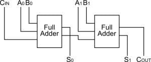
Let’s look at an adder circuit which every microprocessor includes. The diagram below shows a 2-bit adder at a functional block level with five inputs: Cin, A0, B0, B1, B2 and three outputs: S0, S1, C0.  Applying a functional test would result in you adding all possible combination of numbers; 2**5 which is 32 test vectors. How, ever there exist only 2*3 possible outputs- 16. Right off the back you can sense an improved efficiency is right around the corner. Applying S@ fault model at the inputs and outputs you have a total of 16 S@ fault models to detect. That though presumes nothing about the contents of each 1-bit adder. What’s inside the box?
Applying S@ Model to a 1-bit Adder
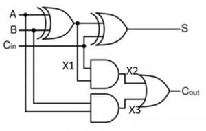
The diagram above has a series of XOR, AND and OR gates. Three internal signals (X1, X2, X3) lie between the adder’s inputs and outputs. To develop a test for a S@ fault you need to know what inputs “pass” the faulty state for detection. In the introductory article we discussed those states for a NAND and a NOR gate. You get to revisit this concept as we proceed to propagate a fault to an output.
Let’s first look at the Cin signal and work at propagating the impact of a S@1. Cin is the input to an XOR circuit and a AND circuit.
For the XOR circuit an X1 value of either “1” or “0” will let you detect a faulty Cin. It’s nice to have choices; let’s choose “1.” For A and B to create a “1” either “10” or “01” will give you that state. You choose the A and B values. With Cin S@1 you detect the fault at S because you observe a “0” instead of a “1.”
Another Observation Point for Cin Faults
You can now check on propagating Cin S@1 to the Cout signal. You have an AND gate;1 X1 needs to be a “1” to pass Cin’s value to the next gate. Lucky you, you already know how to do that (AB = “01” or “10”). However, you have another set of gates to control so that you can observe a faulty response at Cout. This maybe where things get a little tricky.
With Cin S@1 and X1 =“1”, X2 = “1”, you would expect a “0” if Cin = “0.” For you to pass the X2 value to Cout you need X3 to be a “0.” Then faulty response will be Cout=1 the good response will be Cout=0.
How to get that 0, you have choices AB can be “00”, “01” or “10.” Ut-oh- here’s the tricky part is there a conflict? Between deriving X1 and deriving X2 from the same values A and B—turns out you can. In combinational logic you can run into logic conflicts when attempting to propagate a fault state to your observation point. Can you find such a conflict in looking at the other S@ faults for this 1-bit adder?
Learnings from the 1-Bit Adder
In walking through this 1-bit adder you have taken fault propagation through several states. You learned that in combinational logic one can have multiple states to propagate a fault. You also have a passing glance at conflicts. Finally, you can probably gain an appreciation for why engineers built simulators to perform the tedious task of fault simulation.
In the next article we will look at a 2-bit adder circuit to make some observations regarding hierarchy, larger building block assumptions and how knowledge about the black box results in efficient testing. Meanwhile, do you work with circuitry at the black box level that you would like to know more about. Let me know in the comments below and I’ll give you some references to unveil your black box from a test perspective.
Meanwhile remember testing takes time and thoughtful application,
Anne Meixner, PhD
Additional Reading:
To learn a bit more about adders check out this article. Want to know the full truth table for a 2-bit adder- see here.
Professor Ed McCluskey wrote a classic text book on VLSI logic design that included lots of test information. While there exist more recent books on testing, I believe this one provides a great primer on the topic.
I met Ed during my PhD studies while attending the International Test Conference. While he had a reputation for being cantankerous I found him to be approachable. To attend a corporate party at ITC one time I masqueraded as him while my Intel co-worker Dave Zimmerman went as Mrs. McCluskey. I believe Ed would have fully approved our party crashing technique.

 Ask a question or send along a comment.
Please login to view and use the contact form.
Leave a Reply