
In a previous article I alluded to Design for Test (DFT) by mentioning a specific example.
The techniques have been around for decades. Just how long ago though?
I searched on “Design for Test” in the IEEE paper data base; the search resulted in 760 references the oldest being 1983.
Hmm there had to be earlier papers? So next I plugged in the key words “Design For Testability.” This time a list of 4,235 references appeared, the oldest one published in 1978.
LSI Chip Design for Testability provides one of the earliest descriptions of a deliberate and systematic method for increasing an integrated circuit design’s testability. Written by S. DasGupta, E. Eichelberger, T. Williams, their paper describes an approach used at IBM. Large Scale Integration (LSI) refers to having thousands of transistor on a single silicon semiconductor microchip. In the mid 1970’s computer makers developed computer processor microchips and in turn the manufacturing test challenges for these devices loomed. IBM engineers used level scan based design to solve their test challenge.
So What Does Design for Test Mean?
Well, depends upon the engineer you ask. Fundamentally, DFT consists of modifications to the chip or circuit design that make the design easier to test. Such modifications vary upon your goal in making things easy.
Consider one of the following “making things easy” goals:
- Predictability of test results, i.e. no unknowns
- Observability- ability to know the state of internal nodes
- Faster application of testing
- Facilitate fault propagation
- Automatic testing- press a button, wait, check results
- Improved test coverage- your choice of fault model
Engineers apply DFT techniques to digital, analog and memory test. Methods are generally split in to two categories- Ad Hoc and Structured methods. For the rest of this article I will use digital circuit examples to illustrate.
Ad-Hoc Methods
Ad-hoc DFT methods typically consist of lists of either “don’t” or “do” rules for VLSI design engineers. Such rules can be written down and provided to a designer. The rules guide a designer to make a deliberate design choice that helps test.
As noted in How to Test Clocked Circuits– it’s not good to have asynchronous sequential circuits as you can’t easily control its power on state. So adding circuity to make them have a known value addresses predictability (in the DFT castle this is more often referred to as controllability).
Another example can be limit gate fan-in and fan-out. First why is this a good rule? If you are attempting to propagate faults limiting the paths in and out of a logic gate makes this task easier.
You can educate the designer on testability. However, it’s a very manual/human involved process. This also makes it hard to check that a design has followed all the ad-hoc rules. Typically, this would be done in a design review in which experienced engineers are present. though software to audit a design’s adherence is not unheard of.
With hundreds of transistors, maybe even 1000’s of transistors a design review is plausible. Once you reach 10,000’s or 100,000’s of transistors you might want something more structured. This enables software to both create the DFT and check that it was done correctly.
Structured Methods
What do you think of when you read the word structured?
Something built. In the case of DFT its adding circuitry just for test purposes.
In the DFT castle two characteristics are often seen in structured DFT. Just like ad-hoc methods this is about a deliberate design choice to facilitate testing. However, this choice necessitates adding circuits, interconnect and sometimes pins that only exist for test purposes. Second, it’s a systematic top-down approach for which can be applied across the whole chip design. This also enables electronic design automation systems (EDA) to add the circuitry as well as verifying the goals for test quality and test time have been met.
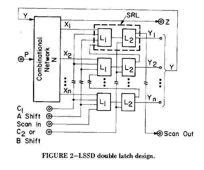
In digital testing the most common structured method is scan-based design. Recall the IBM paper from 1978 discussed earlier. Generically a scan design takes a computer chip design’s flip-flops, modifies the flip-flop design and converts them into a connected shift register which permits you to control the states for test. You can also observe them.
The modified flip-flop from the IBM paper looks like this.
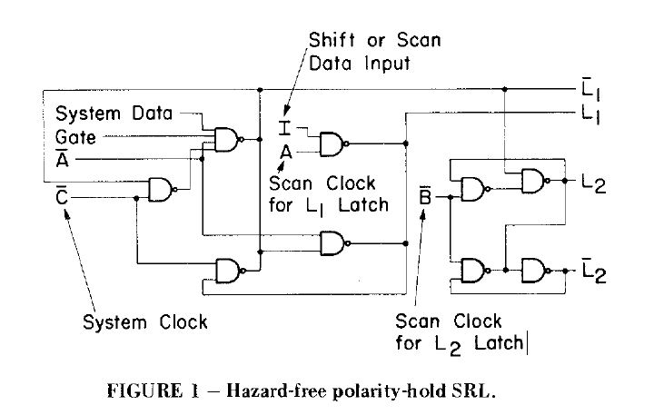
It looks generically like the figure below (from the IBM paper).
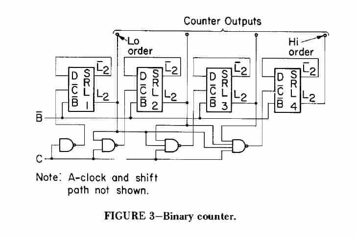
Examples of how one modifies a binary counter the paper also provided.
For digital circuits it means adding extra logic and signals dedicated for test according to some procedure. That means the circuitry has two modes- normal or mission mode and test mode.
An on-chip pattern generator provides another structural DFT test method. You add circuitry which generates the tests and typically you provide a way to check it on-chip. It falls under DFT Castle wing called Built In Self-Test (BIST).
So What Does Design for Test Involve?
First, it involves choices- what approach are you going to take, what test goals do you want to accomplish and what are you willing to pay for in terms of implementation
Second, it involves design- implementation and verification that it meets your goals.
Third, it involves application—in a manufacturing setting the tests use the DFT.
As mentioned in the previous article there’s a HUGE castle for DFT in which there are many techniques and choices especially when it comes to the trade-offs on implementation costs (e.g. area overhead) versus test time versus quality goals. Plenty of building blocks to consider when considering the application side of DFT. You will be going further into the castle in future articles.
Does this primer satisfy your needs for an overview of DFT? Let me know in the comments.
Meanwhile remember testing takes time and thoughtful application,
Anne Meixner, PhD
Tags: Mastery 1, Design For Test, Scan, Digital testing
Additional Reading:
Professor Mark M. Tehraniapoor (University of Florida) has a good set of slides on DFT and an introduction to Scan.
The oldest paper found with a search on “Design for Test” is dated 1983. While at General Electric D. K. Bhavasar wrote “Design for Test Calculus: An Algorithm for DFT Rules Checking.” The abstract is below. I met Dilip Bhavsar when I began regularly attending the International Test conference as an Intel engineer. Dilip worked at Digital Equipment Company, DEC, and eventually through separation and acquisition Dilip and I both worked for Intel.
A new one-pass algorithm for checking networks for compliance to a set of Design for Test (DFT) rules is presented. The algorithm is based on a “Design For Test Calculus” which defines various types of signals and nodes in the network, signal sets attached to node’s inputs and outputs, and rules for transferring signal sets through nodes. The rule checking is accomplished by examining the characteristic contents of the signal sets transferred. The calculus is capable of handling a wide variety of “test point flip-flops” and test access schemes, and has features that make hierarchical rule checking feasible.

Leave a Reply